Laser MBE
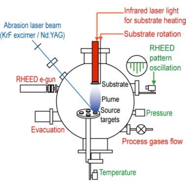
The laser MBE is a refined method of PLD that realizes epitaxial growth of various oxide/nitride thin films on a substrate. In laser MBE a substrate and sintered targets are set in an ultra high vacuum (UHV) chamber as shown in Fig.1. Epitaxial growth is caused by ablation of source target by irradiation of laser pulse and sticking/coverage to growing surface on the substrate.
The laser pulse is introduced from outside UHV chamber through a quartz window.
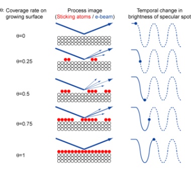
The growth process can be monitored in situ by RHEED of which intensity oscillation is interpreted by an elastic scattering model shown in Fig.2.


Advantages of our system are;
- Easy evaporation despite materials with high melting point (ex. oxides).
- Little difference of chemical composition between source targets and deposited films.
- Quite few contamination due to laser abrasion as a light-induced process.
- Digital (or discrete) control of film thickness/growth rate by repetition number of the laser pulse.
- Growth under wide-vacuum-range condition with process gas flow is acceptable.
- Easy exchange of targets that leads to realize heteroepitaxy and multilayered structure.
The laser MBE is very suitable for the atomic layer controlled growth of oxides/nitrides, and also suits for a simple and inexpensive apparatus comparing with conventional MBE.
Our laser MBE system pursues extremely to be compact, and contains many outstanding know-hows on, for instance, the substrate heating and the load-locked exchange of samples or targets.
The laser MBE has advantages of both the conventional MBE and the pulsed laser deposition (PLD), simultaneously, because the deposition method means a pulsed laser abrasion growth in an ultra high vacuum circumference.
Combinatorial method for material science
Synthesizing at one time specimens representing all combination of synthesis conditions concerned followed by screening the products features the "combinatorial chemistry", which becomes indispensable now in medicine or pharmaceutical development. As a result of the combinatorial chemistry, an "exponential" acceleration of development speed has been proven.
Why don't you get the scheme in your thin film study? From an early stage of the scheme we have been developed "combinatorial PLD apparatuses" with an academia. Our experience can help your thin film research and development!
Application to oxide electronics
Molecular layer epitaxy of oxides is expected to contribute to the future electronics, for instance,
- Ultimate Silicon electronics
- Quantum effect electronics
- High temperature supercondutor electronics
- Whole epitaxial oxides electronics
Application to novel thin film and their device technology
Our apparatus is also applicable to a wide variety of thin film growths ranging from nitrides like GaN to organic thin films and to junction device fabrivation such as diamond, Fullerene, and Silicon junction with oxides.
